Dive Brief:
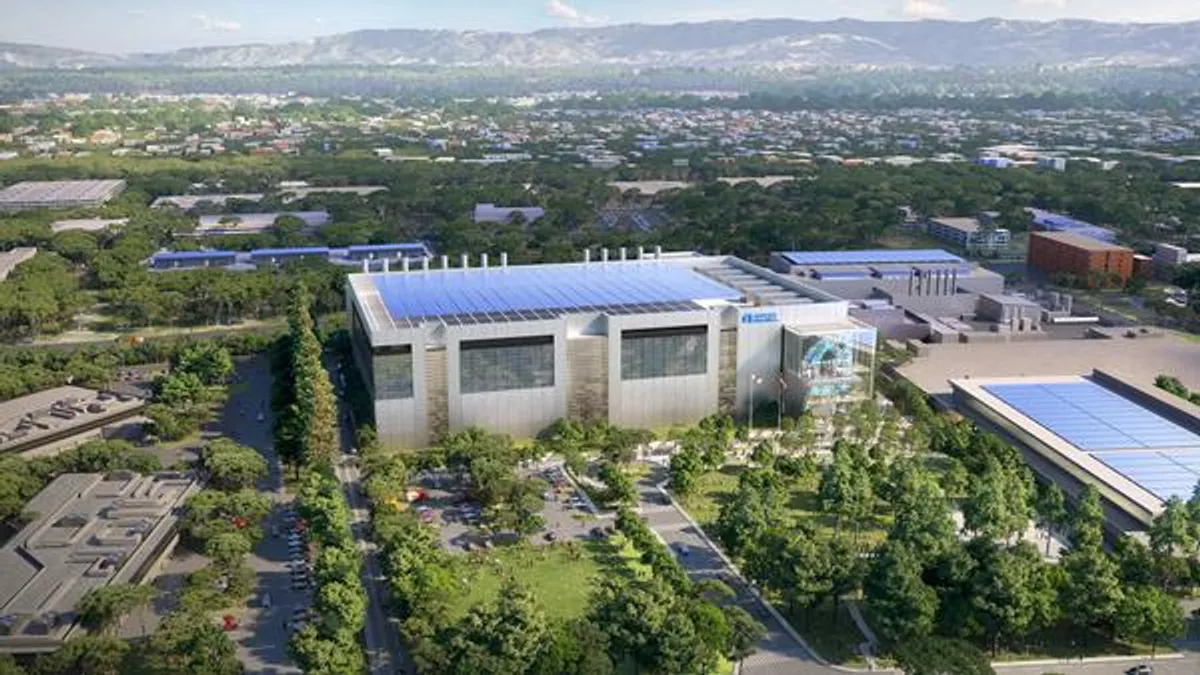
- Semiconductor toolmaker Applied Materials announced plans to invest up to $4 billion on a Silicon Valley research center to spur advances in semiconductor manufacturing on Monday.
- The new Equipment and Process Innovation and Commercialization (EPIC) Center, encompassing over 180,000 square feet, will offer chipmakers a dedicated space within the facility for pilot design work, including early access to next-generation processes and equipment.
- Applied Materials expects the center, which is slated for completion in 2026, to house more than $25 billion of company research work in its first decade.
Dive Insight:
The announcement comes as the federal government begins to deploy nearly $53 billion in funding earmarked for U.S. chip development as part of last year’s CHIPS and Science Act. Applied Materials noted that the scope of its project investment is contingent on receiving funds from the act.
The company’s new center is expected to cut the time it takes the industry to bring a new technology to market by several years, helping to meet the rising demand for chips.
“While semiconductors are more critical to the global economy than ever before, the technology challenges our industry faces are becoming more complex,” President and CEO Gary Dickerson said in a statement. “This investment presents a golden opportunity to re-engineer the way the global industry collaborates to deliver foundational semiconductor process and manufacturing technologies needed to sustain rapid improvements.”
U.S. Vice President Kamala Harris is set to attend an Applied Materials event announcing the center at its California headquarters on Monday, along with executives from major chip companies.
Harris will deliver remarks on how the CHIPS and Science Act is sparking domestic investment in advanced semiconductor manufacturing, according to the White House.


